2
RF Device Data
Freescale Semiconductor
MRF5P20180HR6
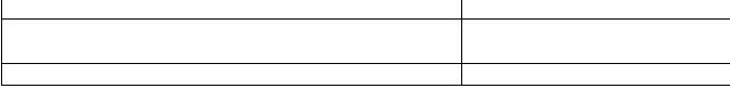
Table 3. ESD Protection Characteristics
Test Conditions
Class
Human Body Model
2 (Minimum)
Machine Model
M3 (Minimum)
Charge Device Model
C7 (Minimum)
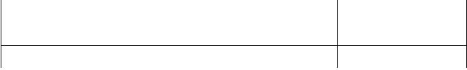
Table 4. Electrical Characteristics (TC
= 25
°C unless otherwise noted)
Characteristic
Symbol
Min
Typ
Max
Unit
Off Characteristics (1)
Zero Gate Voltage Drain Leakage Current
(VDS
= 65 Vdc, V
GS
= 0 Vdc)
IDSS
?
?
10
μAdc
Zero Gate Voltage Drain Leakage Current
(VDS
= 28 Vdc, V
GS
= 0)
IDSS
?
?
1
μAdc
Gate-Source Leakage Current
(VGS
= 5 Vdc, V
DS
= 0 Vdc)
IGSS
?
?
1
μAdc
On Characteristics
Gate Threshold Voltage
(1)
(VDS
= 10 Vdc, I
D
= 200
μAdc)
VGS(th)
2.5
2.7
3.5
Vdc
Gate Quiescent Voltage
(3)
(VDS
= 28 Vdc, I
D
= 1600 mAdc)
VGS(Q)
?
3.6
?
Vdc
Drain-Source On-Voltage
(1)
(VGS
= 10 Vdc, I
D
= 2 Adc)
VDS(on)
?
0.26
0.3
Vdc
Forward Transconductance
(1)
(VDS
= 10 Vdc, I
D
= 2 Adc)
gfs
?
5
?
S
Dynamic Characteristics
(1,2)
Reverse Transfer Capacitance
(VDS
= 28 Vdc
±
30 mV(rms)ac @ 1 MHz, V
GS
= 0 Vdc)
Crss
?
1.7
?
pF
Functional Tests
(3)
(In Freescale Test Fixture, 50 ohm system) V
DD
= 28 Vdc, I
DQ
= 1600 mA, P
out
= 38 W Avg.,
f1 = 1932.5 MHz, f2 = 1942.5 MHz and f1 = 1977.5 MHz, f2 = 1987.5 MHz, 2-Carrier W-CDMA, 3.84 MHz Channel Bandwidth Carriers.
ACPR measured in 3.84 MHz Channel Bandwidth @ ±5 MHz Offset. IM3 measured in 3.84 MHz Bandwidth @ ±10 MHz Offset. PAR =
8.5 dB @ 0.01% Probability on CCDF.
Power Gain
Gps
12.5
14
?
dB
Drain Efficiency
ηD
23
26
?
%
Intermodulation Distortion
IM3
?
-37.5
-35
dBc
Adjacent Channel Power Ratio
ACPR
?
-41
-38
dBc
Input Return Loss
IRL
?
-16
-9
dB
1. Each side of device measured separately.
2. Part internally matched both on input and output.
3. Measurement made with device in push-pull configuration.


发布紧急采购,3分钟左右您将得到回复。
相关PDF资料
MRF5P21045NR1
MOSFET RF N-CH TO-270-4
MRF5P21180HR6
MOSFET RF N-CHAN 28V 38W NI-1230
MRF5P21240HR6
MOSFET RF N-CHAN 28V 52W NI-1230
MRF5S19060MR1
MOSFET RF N-CH 28V 12W TO-270-4
MRF5S19060NBR1
MOSFET N-CH 12W 28V TO-272-4
MRF5S19090HSR5
MOSFET RF N-CHAN 28V 18W NI-780S
MRF5S19100HSR5
MOSFET RF N-CHAN 28V 22W NI-780S
MRF5S19130HSR5
MOSFET RF N-CHAN 28V 26W NI-880S
相关代理商/技术参数
MRF5P20180HR6_06
制造商:FREESCALE 制造商全称:Freescale Semiconductor, Inc 功能描述:RF Power Field Effect Transistor N-Channel Enhancement-Mode Lateral MOSFET
MRF5P20180R6
制造商:MOTOROLA 制造商全称:Motorola, Inc 功能描述:RF POWER FIELD EFFECT TRANSISTOR
MRF5P21045NR1
功能描述:射频MOSFET电源晶体管 HV5 2170MHZ 10W TO270WB4 RoHS:否 制造商:Freescale Semiconductor 配置:Single 晶体管极性: 频率:1800 MHz to 2000 MHz 增益:27 dB 输出功率:100 W 汲极/源极击穿电压: 漏极连续电流: 闸/源击穿电压: 最大工作温度: 封装 / 箱体:NI-780-4 封装:Tray
MRF5P21180
制造商:FREESCALE 制造商全称:Freescale Semiconductor, Inc 功能描述:RF Power Field Effect Transistor
MRF5P21180HR5
功能描述:射频MOSFET电源晶体管 HV5 38W WCDMA NI1230H RoHS:否 制造商:Freescale Semiconductor 配置:Single 晶体管极性: 频率:1800 MHz to 2000 MHz 增益:27 dB 输出功率:100 W 汲极/源极击穿电压: 漏极连续电流: 闸/源击穿电压: 最大工作温度: 封装 / 箱体:NI-780-4 封装:Tray
MRF5P21180HR6
功能描述:射频MOSFET电源晶体管 HV5 38W WCDMA NI1230H RoHS:否 制造商:Freescale Semiconductor 配置:Single 晶体管极性: 频率:1800 MHz to 2000 MHz 增益:27 dB 输出功率:100 W 汲极/源极击穿电压: 漏极连续电流: 闸/源击穿电压: 最大工作温度: 封装 / 箱体:NI-780-4 封装:Tray
MRF5P21180HR6_08
制造商:FREESCALE 制造商全称:Freescale Semiconductor, Inc 功能描述:RF Power Field Effect Transistor
MRF5P21180R6
制造商:MOTOROLA 制造商全称:Motorola, Inc 功能描述:RF Power Field Effect Transistor